Custom Printed Circuit Boards
![]()
![]()
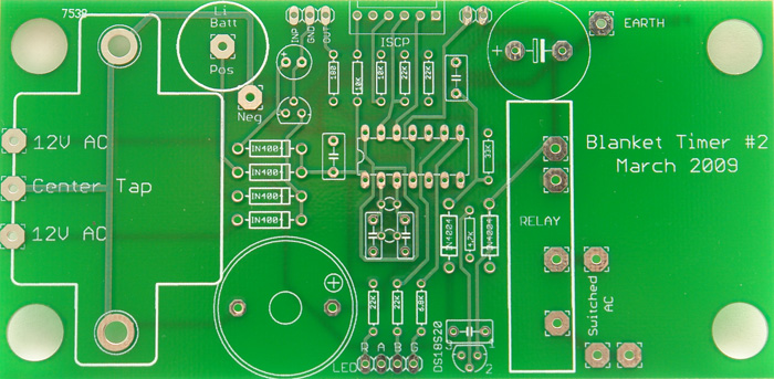
![]() Creating your own, professional quality printed circuit boards, is not as hard, or as expensive, as you would think. There is a lot of good software out there and any number of PCB fabrication houses who are eager for your business, even though it is only one PCB that you want.
Creating your own, professional quality printed circuit boards, is not as hard, or as expensive, as you would think. There is a lot of good software out there and any number of PCB fabrication houses who are eager for your business, even though it is only one PCB that you want.
You could still etch and drill your own board, and that would be great if you like wearing horsehair shirts. But this is the Internet era - just send off your design and get a professional result back.
This article is aimed at the hobbyist who wants a custom PCB for their latest creation and does not want to pay the earth. It summarises one approach to creating the perfect PCB. If you are keen you can find other software and PCB houses, but this method works for me.
The Software
A modern software package is vital to producing a good looking PCB. Using this you can enter the circuit, then design the board to match the circuit and finally export the instructions for the machines that will make the board.
Previously I used Eagle from Cadsoft for this job but these days it is very old and clunky..
There are many excellent and free replacements available but, for a beginner, I recommend easyEDA (https://easyeda.com). The standard edition operating entirely online will do everything a normal user (or even a professional) would need and is very easy to use.
The best feature is that the standard edition is free and is guaranteed to remain free. Also, there are no stupid restrictions (unlike Eagle).
The following is a simple overview of the process using easyEDA. However you will still need to follow their tutorials and check their documentation to get a good result. This YouTube playlist also provides a good introduction:
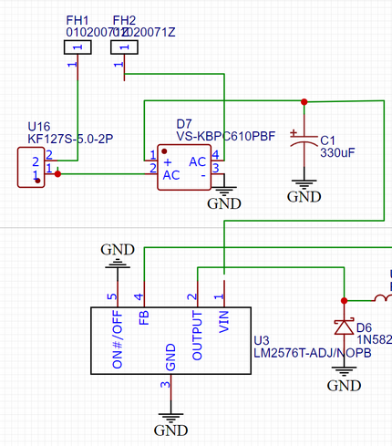 |
The schematic. |
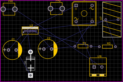 |
| The footprints placed on the board with ratsnest lines. |
Entering the Schematic
All PCB designs start with drawing the schematic. This involves selecting components, dropping them onto the drawing sheet and connecting them.
Each component has a footprint associated with it so that when you transfer the design to a PCB the solder pads will be in the correct place for the physical component.
One of the best features of easyEDA is that it has a huge library of components with accurate footprints so you do not have to create your own - they are there ready to use.
Another handy feature is that the schematic looks reasonably good so you can use it as part of your documentation (as shown on the right).
Creating the Board
With the schematic drawn you can switch to the PCB layout mode. Initially this will show a blank board with the components from your schematic arrayed off to the side of the board as footprints. Using your mouse you can drag these onto the board, rotate them and place them where you like.
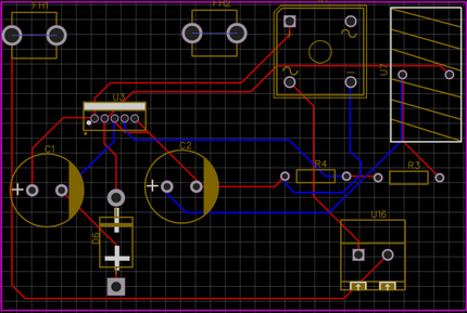
The connections between these components is depicted as a series of faint blue lines called a ratsnest(as shown on the right). The next step is to draw the copper tracks between the components replacing the ratsnest lines.
As you draw you can select the top or bottom of the PCB for the track and the track width.
When you have finished you can use easyEDA to check that there are no errors. These could be unconnected components, tracks that are too thin, tracks too close to each other and so on.
EasyEDA will also show you a realistic 3D image of the final board. This can be rotated and zoomed and is invaluable for making sure that the component spacing is reasonable and that the silk screen printing is legible.
 |
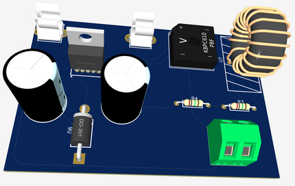 |
| Now the copper tracks have been drawn replacing the ratsnest lines. | One of the handy features of easyEDA is that it can show you what your finished board will look like. |
Exporting the Design
The final step is to export the design as Gerber files (see this explanation of Gerber files). These can be sent to any fabricator who will make the PCB for you. However, before you do that, you should use a Gerber viewer to check exactly what the fabricator will be making. I recommend gerbv (link) for this task.
Using the Gerber viewer check each layer in detail to make sure that there is sufficient clearance, tracks are complete, etc. It is amazing the defects that can be found in this final step.
PCB Design Tutorial
David L. Jones has created an excellent tutorial on the ins and outs of PCB design. His paper can be downloaded from his website http://www.alternatezone.com/electronics/pcbdesign.htm.
PCB Fabrication
The Gerber files can be sent to almost any modern PCB fabricator who will make the board and send it back to you. .
The best part of modern PCB fabrication is the fact that it is so easy - you just send off your design via the Internet and back come the boards. No drilling, cutting, chemicals and mess. The bad part is that it takes a few weeks before you get them in your hands.
I use JLCPCB and I am happy to recommend them and easyEDA (which is associated with JLCPCB) make it easy to transfer the files to them for ordering. However, there are many other fabrication houses that you can use (as Goggle will show you).
JLCPCB's prices are good, they are fast and they have some cheap freight options. For a small board they charge a ridiculously cheap price of US$2 (plus freight) and you will get five boards for that price. For a more reasonable sized board of 10cm x 20cm they are still very cheap at US$12 plus postage for five boards. All prices were correct as at May 2023.
Not bad for a professional quality double sided PCB with plated through holes, solder mask on both sides, and silk screen printing on both sides. You could not get better if you were IBM.
Using this technique you will have a board that you can be rightly proud of...
